Call Us: 858-784-0900
Email Us: Sales@ACETEC.com

Author: Mark Hoffman

Mark Hoffman No Comments

Datalink Range Improvement

One of the most important factors to consider when developing a communication datalink range is the ability to provide sufficient signal strength out to the intended operational range of the platform. Modern radios provide a starting point for this effort as they provide options such as programmable bandwidths, RF power settings and modulation based on the application. Output powers of up to 2 watts provided by these radios offer a great foundation for transmissions over short distances, but as either the range or data rates increase, the effectiveness of this output begins to degrade and may even result in the loss of the datalink.

Power Amplifier for Datalink Range Communications


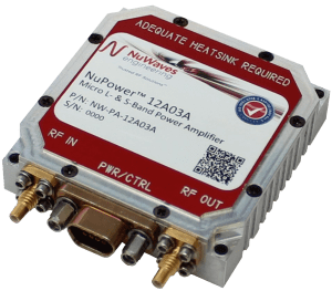
Figure 1: NuWaves NuPowertm Micro L & S Band Power Amplifier


If the application requires either increased range or data rates, the designer is left with two options. One is to improve the performance of the antenna through the use of exotic antenna designs. Unfortunately, many applications are limited to simpler omni-directional systems out of a need to meet operational requirements such as flight envelopes. The second option is to utilize an RF power amplifier. Amplifiers can provide increased data throughput and range, both with and without the use of specialized antennas. Augmenting the transceiver through the integration of an amplifier allows the designer to overcome the impact of such things as free space propagation path loss, insufficient antenna gain, and when paired with a LNA can result in increased receiver sensitivity. Every 6 dB increase in SNR results in the doubling of the effective range of datalink, meaning that an amplifier that can combine high power output, small size, and electrical efficiency can be an ideal solution for applications such as man or vehicle portable communications links and Un-Manned Aerial Systems.

NuWaves Engineering has developed a wide variety of off-the-shelf RF amplifiers with rich features to support mission-critical CONOPS in telemetry, ISR, and tactical communication systems applications to handle all of your datalink range needs. Frequency ranges are available from UHF through C-band with output power levels ranging from 5 to 100 WAll NuPowerTM PAs and NuPower XtenderTM BDAs are designed, built and tested in-house under NuWaves’ Quality Management System (QMS) certified to AS9100:2009 and ISO 9001-2008 standards, which ensures that each product arrives on-time and defect-free. Most models are in-stock, and are available for same-day shipment on orders placed before 2pm. NuWaves also boasts a full suite of state-of-the-art design and simulation tools, test and measurement equipment, prototyping equipment and a full-scale production facility to provide custom solutions to your specifications. Contact NuWaves today to extend the range of your communications systems and don’t forget to check out our RF Amplifiers and Frequency Converters. – by Ryan Foster Nu Waves Engineering

Mark Hoffman No Comments

Do You Need a Go-To Amplifier?

As a radio designer, it’s nice to have a go-to amplifier that you can use and reuse for a wide range of application frequencies, linearity requirements, bias voltages and currents. The GRF2013, part of Guerrilla RF’s standard DFN-6 portfolio, is a device that you can turn to over and over again for a wide variety of requirements.


Key Strengths of GRF2013:

  • Outstanding RF performance  over a wide range of bias conditions
  • Flexible biasing: Vdd can range over 2.7 to 5.0 volts with Iddq adjustable from 15 to 100 mA
  • Internally pre-matched to 50 ohms. A single set of external components yields multi-octave bandwidths from 50 MHz to 4 GHz and beyond
  • Automotive qualification coming soon
  • Part of GRF’s 1.5 mm DFN-6 portfolio, which offers over 20 devices using the same package, pin out, and layout

The GRF2013 data sheet focuses on 700 to 3800 MHz performance at 5.0 volts and 90 mA Iddq. However, this amplifier also excels below 1 GHz with a 3.0 volt power supply (see charts below). Notice the flat gain, NF and linearity over the measured 200 to 500 MHz band.

GRF2013 is in full production and is pin/layout compatible with more than 20 devices using our standard 1.5 x 1.5 mm DFN-6 plastic package. Evaluation boards and samples are available now.

Guerrilla RF is committed to providing the high performance RF solutions you need in the long term, and we will be pleased to provide the applications support you need to successfully implement any of our devices. –  by Guerrilla RF


Mark Hoffman No Comments

How to Decrease EMI and Increase Radio Range?

Electromagnetic interference (EMI) reduces radio range, drastically decreasing the functionality of Internet of Things products. There are some local and intermittent EMIs that are eventually get addressed, thanks to the Wi-Fi protocols that come complete with automatic retry features. However, the interference coming from external sources are continuous in nature and can drastically reduce the range of a device’s onboard radio. This kind of interference has to be addressed by the right mechanical and PCB design. But what about the interferences that come right from your own product?  Here are some useful tips that will help you minimize the EMI being emitted by your product and improve radio range:

PCB Shielding

Metal shields isolate circuits and prevent interference from reaching the antenna. At the same time, the antenna needs to be present outside the shield for receiving signals. So, shielding the interference sources is a better option than shielding the receiver. The Faraday cage is the best shielding solution available that provides a conductive box without any seams around the shielded circuitry.

However, you must develop metal shields with minimal contact resistance. And, there are several options to achieve this:

  • Pick clear chromate instead of aluminum as it provides decent conductivity while resisting corrosion.
  • Use an overlapping structure for an increased area and decreased contact resistance.
  • Minimize contact resistance through gaskets that rely on screws outside the gasket for more reliable contact and compression force.

Select the Right Clock Frequencies

Certain circuits are never switched off, and the resulting interference affects the receiver’s sensitivity. In a controller board, for example, clock oscillator signal harmonics cannot be controlled easily and lead to interference. There is one clock of 19.2 MHz and another of 25 MHz in a Raspberry Pi design. While the latter falls between the popular non-overlapping Wi-Fi frequencies, the former falls inside the Wi-Fi frequency channels. So, even though the 25 MHz clock doesn’t solve the interference issue entirely, it does help to a certain extent.

Check for EMI Issues

Detecting interference issues becomes easier with a spectrum analyzer. Select one that has greater maximum frequency than the system radio’s highest frequency. When an antenna probe is connected to this analyzer, it can detect design problems and locate interference sources. No wonder this setup is used by the FCC to test for EMI compliance and radio performance issues.

Switching up the components of a PCB can work wonders when it comes to decreasing EMI interference and improving radio range. Sure, it’s better if you detect all the problems as early as possible, but it’s worth noting that following the steps above can result in a design that minimizes EMI emission and prevents interference from affecting other parts of the radio system. To know more about EMI shielding, click here. -LeaderTech

Mark Hoffman No Comments

How to Ensure Corrosion Resistant EMI Protection

EMI shielding products are designed to protect electronics from the effects of interfering energy waves. But what happens when you use your equipment in an extremely damp environment? In such a situation, your priority should be to make your EMI shielding products corrosion-resistant. Rust or material deterioration will affect device performance due to high-frequency emissions interfering with your electronic gadgets. Here are a few ways to protect your equipment from corrosion:

Consider Surface Treatment

Paint or plate your electronic enclosures. It is essential to prevent corrosion, oxidation, rusting, and tarnishing. Maintain application aesthetics. When it comes to the flange surfaces, they require finishing for maximum protection against corrosion. There are a few factors to consider when employing finishing. You must ensure maximum shielding efficiency through corrosion-resistant and electrically conductive materials. You will require an additional coating for protecting shielded products from being corroded in high humidity surroundings.

Pick out Quality EMI Gaskets

Choose the right gasket material that can cut back the variation in electrochemical potential in relation to the metal structure. It helps to decelerate the corrosion process through a lower galvanic current. Opt for elastomeric gaskets that come with filler particles. The material will ensure both corrosion resistance and EMI shielding when exposed to metal. Use silver-plated copper, pure silver, and silver-plated aluminum fillers to ensure corrosion resistant EMI protection.

Opt for Additional Moisture Sealing

Spray or salt fog acting as an electrolyte may corrode your shielding materials. This is the reason why designers require secondary moisture sealing to get rid of it. To prevent corrosion in aircraft applications, a seal-to-seal design is the preferred choice of EMI shielding engineers. Similar gasket materials are used in every mating flange. Non-conductive sealers are used to stop water from seeping into your shielded products.

Choose the right EMI gasket material for protection against water, fog, or salt spray. The use of conductive coating and an additional moisture seal will keep corrosion under control for improved shielding effectiveness. If you want to learn more about our products, contact us today. -LeaderTechInc.com

Mark Hoffman No Comments

pSemi Releases World’s First, Fully Integrated, 8-channel LED Boost

Power Supply in Package (PSiP) Uses a Unique Design Based on a Patented, Two-stage Architecture that Relies on Capacitors to Handle the Bulk of the Power-conversion Work

SAN ANTONIO – APPLIED POWER ELECTRONICS CONFERENCE (APEC) – March 6, 2018 – pSemi Corporation (formerly Peregrine Semiconductor), a Murata company focused on semiconductor integration, introduces the PE23300, the industry’s only fully integrated LED boost power supply in package (PSiP) based on a charge-pump, switched-capacitor architecture that offloads most of the power-conversion work from the inductor to capacitors in the charge pump.

Powering up to eight LED strings at a total power level of up to 10 watts, the PE23300 is designed specifically to power LED backlight arrays in ultra-high-definition (UHD) and high definition (HD) LCD panels for 2-cell and 3-cell narrow-voltage DC notebooks, industrial and automotive displays.

PE23300 Fully Integrated 8-channel LED Boost

“The PE23300 truly demonstrates pSemi’s power-semiconductor capabilities. The PSiP delivers a unique, two-stage architecture that brings ground-breaking conversion efficiency and small solution size and is packaged with Murata’s advanced, 3D-packaging technology and passive components,” says Stephen Allen, director of strategic marketing at pSemi. “All components required for operation are integrated into a 7.7 x 11.7 millimeter laminate-based LGA package, which is just 1.6 millimeters in height. To achieve this small size, we used a ‘die-in-substrate’ 3D-packaging technology. The low profile is also a result of our two-stage architecture that allows us to use a tiny chip inductor. All of this can be achieved with an efficiency that is on average about 5 to 7 percent higher than the competition, halving the losses in the LED boost.”

Power conversion creates a compromise between size and efficiency: The smaller the solution, the worse the efficiency. This compromise impacts OEMs trying to make next-generation, ultra-compact products, because they need both a very high conversion efficiency and a very small size at the same time. pSemi solves this problem with a novel, two-stage architecture that offloads most of the power-conversion work from the inductor to a virtually lossless charge pump and relies on small, multilayer ceramic capacitors (MLCCs) to do most of the work. As a result, the inductor – usually the largest and tallest component – can be reduced dramatically in size, and traditional wire-wound inductors can be replaced with chip inductors. This patented architecture was first developed by Arctic Sand Technologies, an MIT spin-out acquired by pSemi in March 2017, and commercialized this year.

Beyond the smaller inductor and higher efficiency, this architecture delivers several other key benefits for LED boosts, including full short-circuit protection and a very flat efficiency over the entire load range. Also, efficiency is virtually independent of the output voltage, and this allows more LEDs per string. With fewer strings, efficiency is optimized, and the display-bezel size can be reduced in width. pSemi’s PE23300 features low power dissipation – up to half that of competing products – that improves reliability and supports portable applications’ extensive battery run times.

Product Features

The PE23300 features an input voltage range of 4.5V to 15V DC and powers up to eight strings of LEDs at up to 45V and 40 mA per string.

The PSiP provides full programmability via an I2C interface with settings stored in non-volatile memory or by using GPR pins. Dimming resolution is up to 12-bits resolution with an additional 3-bit dithering and can be either linear/logarithmic analog and PWM dimming or direct PWM dimming for maximum flexibility and resolution. The part features an LED brightness ramp up/down control with programmable ramp rate, linear/logarithmic ramp profiles and phase-shifted PWM dimming among active strings to minimize audible noise.

About pSemi 

pSemi Corporation is a Murata company driving semiconductor integration. pSemi builds on Peregrine Semiconductor’s 30-year legacy of technology advancements and strong IP portfolio but with a new mission: to enhance Murata’s world-class capabilities with high-performance RF, analog, mixed-signal and optical solutions. With a strong foundation in RF integration, pSemi’s product portfolio now spans power management, connected sensors, optical transceivers antenna tuning and RF frontends. These intelligent and efficient semiconductors enable advanced modules for smartphones, base stations, personal computers, electric vehicles, data centers, IoT devices and healthcare. From headquarters in San Diego and offices around the world, pSemi’s team explores new ways to make electronics for the connected world smaller, thinner, faster and better. To view pSemi’s semiconductor advancements or to join the pSemi team, visit www.psemi.com.

###

The Peregrine Semiconductor name, Peregrine Semiconductor logo and UltraCMOS are registered trademarks and the pSemi name, pSemi logo, HaRP and DuNE are trademarks of pSemi Corporation in the U.S. and other countries. All other trademarks are the property of their respective companies. The pSemi website is copyrighted by pSemi Corporation. All rights reserved.

Top