Mark Hoffman No Comments

What makes for a perfect Low Noise Amplifier (LNA) MMIC for your microwave system? The answer could be right under your noise figure.

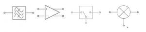
Low Noise Amplifiers (LNAs) are a critical component in virtually all radar, wireless communications and instrumentation systems. But while the noise figure (NF) performance is often your primary focus, other microwave system considerations related to performance and size, weight, power and cost (SWaP-C) can be equally, if not more important. In this blog we’ll describe a few other key characteristics that may help you save time during your design cycle, save money during assembly, and even enhance your microwave assembly or subsystem at-large.

1. Input Power Survivability
Specifically in military and aerospace radar and communications applications, where electronic countermeasures (ECMs) may be used to overwhelm a receiver, a receiver must be capable of withstanding high levels of input power for varying intervals of time. Active or passive jamming can cause levels of noise and frequency bursts that couple large amounts of broadband or frequency-selective interference into a receiver. Moreover, in these applications there is often a high-power transmitter in close proximity to the receiver, which can lead to substantial coupling and power ingress into the receiver front end.

A common method to reduce the impact of critically high input powers to a receiver is to include a limiter or circulator on the input of a receiver chain. An unfortunate side effect of adding anything prior to the LNA in the receiver is the degradation of the overall system noise figure. These signal chain additions reduce the sensitivity of the receiver, which may shorten communications range, throughput, radar range and accuracy, and cause delays in acquiring mission critical information. A great 1 dB system noise figure can effectively become 2 dB or more when adding protection circuitry.

It’s thus very important to consider an LNA’s highest input power handling (or input survivability). Most LNAs can handle only 10-15 dBm pulsed on their input, but the highest achievers are now surviving 20 dBm continuously and 23-25 dBm pulsed and can help you eliminate the protection circuitry.

2. Gain Flatness, and Gain Stability over Temperature
Gain flatness across your required band is essential to achieve required inter-symbol-interference (ISI) levels and optimal range performance. As costly equalizers are often employed to compensate for the downward gain slope of typical LNAs, positive gain slope LNAs reduce that need.

Another factor to consider is gain stability over temperature. In applications such as aerospace communications, and SatCom, operating temperature can exceed 180 degrees F of variation within a short time window.

Temperature changes that are significant can affect an LNA by more than just changing the noise figure of the device and system; they can vary the frequency-dependent gain of the LNA. For example, large-phased array antennas may have thousands of TR modules, with many of the modules exposed to a variety of temperature gradients. If the communications system relies on gain stability throughout the TR modules, and the LNAs gain stability is temperature dependent, the system may suffer a significant loss in performance.

3. Supply Voltage and Power Consumption
Properly biasing a MMIC amplifier is critical to achieving adequate device performance. Depending upon the particular LNA design, the biasing circuitry could be composed of a positive and negative biasing circuit with temperature compensation. Some LNA MMICs have the biasing and compensation circuitry built in, but a positive and negative voltage supply must be provided to the exact specification for the biasing network to operate properly.

When designing at a system-level for a large RF or microwave assembly, many different voltage supplies may be required. Certain design constraints may also limit the noise and stability performance of those power supplies, which may impact the practical LNA performance due to limited power supply rejection ratio (PSRR). To avoid this, additional circuitry may be used to condition the voltage supplies for a given LNA MMIC. Each of these circuits and connection points introduces a potential failure mode to the voltage supplies, and thus impacts system reliability. These supply-voltage circuits also consume valuable assembly real estate and power, contribute to the overall size/weight of the assembly, add costs, and of course, consume design and test time.

In order to reduce the infrastructure necessary to integrate a MMIC LNA into a microwave assembly, engineers at Custom MMIC have applied innovative circuit-design techniques. The designs they have implemented, which only require a single positive voltage supply, also enable a wide range of voltage input for even greater flexibility. All of the necessary circuitry to properly bias these LNAs is integrated into the MMIC itself. Ultimately, when your MMIC requires only a single positive supply voltage it reduces your bill-of-material, overall system complexity, failure modes, and overall system SWaP-C.

In mobile platforms, including aerospace and satellite communications, power constraints are also a system-wide limitation that often dictates what solutions can be used. Moreover, for these applications, the power requirements of the components directly lead to the overall size and cost of the power generation circuits, and hence, the total system SWAP-C. An example of this concept is seen with satellite communications. The power required by a phased-array antenna must be generated by solar cells mounted on the satellite, which is one of the largest contributing factors of satellite weight and size. As launching satellites costs thousands to tens of thousands of dollars per kilogram, reducing the weight of a satellite system can directly influence the cost-per-bit of high-speed satellite communication services.

If your next LNA might find itself in a similar system, be sure its power consumption (bias current and bias voltage) is as efficient as possible. LNAs with lower power needs are also typically smaller, demonstrate better temperature performance, and provide better SNR at lower power levels. –Blog by Custom MMIC

Mark Hoffman No Comments

Breakthrough Ultra Low Noise Amplifier Has 0.6 dB Noise Figure and Covers 2-6 GHz Frequency Range

Breakthrough Ultra Low Noise Amplifier Has 0.6 dB Noise Figure and Covers 2-6 GHz Frequency Range
We’re proud to announce that we’ve recently released a new GaAs Low Noise Amplifier (LNA) MMIC with broadband noise figure performance previously only achievable with discrete FET designs. The CMD283C3, with 0.6dB noise figure, is the first in a family of new Ultra Low Noise Amplifiers.

The CMD283C3 LNA covers 2-6 GHz with high midband gain of 27 dB and output P1dB of 16dBm. The MMIC is housed in a leadless 3×3 mm surface mount package. It operates from a bias supply of +2 to +5 volts and draws a nominal 42mA. The CMD283C3 is ideally suited for S and C band receivers requiring excellent sensitivity, and as a replacement for discrete FET LNA solutions.

Visit https://www.custommmic.com/cmd283c3/for more information and to download full datasheet and S-parameter data. – Custom MMIC

Mark Hoffman No Comments

Rounding up our Best GaN RF Power Amplifier MMICs

The power of GaN MMIC technology is strongest when applied to RF power amplifier MMICs. Here we quickly review some of our power amplifier MMIC successes with GaN.

The CMD262 is a 5 W GaN MMIC power amplifier die ready for Ka-band systems where high power and high linearity are a must. This MMIC amplifier delivers greater than 26 dB gain with a corresponding output 1 dB compression point of +37.5 dBm and a saturated output power of +38.5 dBm at 30% power added efficiency. It is a 50-ohm matched design eliminating the need for external DC blocks and RF port matching.

The CMD216 is a 5.6 W GaN MMIC power amplifier ideally suited for Ku band communications where high power and high linearity are once again crucial. This GaN power amplifier MMIC chip delivers greater than 16 dB of gain with a corresponding output 1 dB compression point of +37 dBm and a saturated output power of +38 dBm at 32% power added efficiency. The CMD216 amp is a 50-ohm matched design also offers full passivation.

The CMD184 is the best rf and microwave power amplifier MMIC chip in its category and is one of our best selling and most popular devices. It is a 4.5 W wideband GaN MMIC power amplifier die which operates from 0.5 to 20 GHz. It delivers greater than 13 dB of gain with a corresponding output 1 dB compression point of +34.5 dBm and a saturated output power of +36.5 dBm. The CMD184 power amplifier MMIC is a 50-ohm matched IC design, eliminating the need for RF port matching. – Custom MMIC

Mark Hoffman No Comments

The Study of Pulse Recovery Times in GaN LNAs: Part II

Building on our previous blog on pulse recovery testing, we present the measurements of pulse recovery time for a commercially available GaN MMIC amplifier with a 5 to 9 GHz bandwidth. The amplifier was assembled into a metal housing, with 2.4 mm connectors used to interface with the test equipment. Three separate units were tested, with the results being consistent among all units. Therefore, we present the results for one unit in the interest of brevity.

We begin by presenting an example of a pulse recovery time measurement in the image above. The interferer pulse is shown in magenta, whereas the desired signal is shown in red. We can see that desired signal is heavily distorted when the interferer is activated, and then recovers once the interferer is disengaged. The recovery is measured as the rise time from 10% to 90% of the signal level.

Next, we observe the pulse recovery times versus input energy under short pulse conditions appears to increase monotonically with increasing input energy, though the relationship appeared to be nonlinear.

We next observed the pulse recovery times versus input energy under long pulse conditions. We note the recovery time increases monotonically with increasing energy, and follows the same trend as the short pulses.

In considering the results for short pulses versus long pulses, we did notice that the recovery time was not solely dependent on the incident energy. Indeed, there were two sets of short pulse and long pulse measurements with the same incident energy, but much different recovery times. Additionally, recovery time vs. energy data is available in our tech brief.

We note that the longer pulses with lower power had a much longer recovery time than the shorter pulses with higher power, even though they had near identical incident energy. Therefore, it appears that pulse recovery time, while being dependent on incident energy, is also dependent on the incident action (energy times duration, uJ-us) of the interfering signal. This is an interesting phenomenon we will explore in future work.

Conclusion 

In this two-part blog series, we presented a methodology for measuring the pulse recovery times of GaN low noise amplifiers in the presence of high power, out-of-band jamming signals. Pulse recovery time is becoming an important metric for assessing system performance. In our examination of a commercially available 5 to 9 GHz GaN LNA, we considered jamming signals that operated under short pulse (< 10 us) and long pulse (> 100 us) conditions. We found that in each case, the recovery time was mathematically related to the input energy through a radical relationship. However, the pulse recovery time also appears to be a function of the input action (uJ-us), as short and long pulses with the same incident energy had recovery times that were different by an order of magnitude. In the future, we will explore this phenomenon through more measurements of GaN low noise amplifiers.  Article by – Custom MMIC

To review additional test data, and to view the complete findings together, download our tech brief: Understanding the Phenomenon of High-Power Pulse Recovery in GaN LNAs.

Mark Hoffman No Comments

pSemi Introduces Family of Switch + LNA Modules for 5G Massive MIMO Base Stations

Ideal for Sub-6 GHz Remote Radio Units, the Front-end Modules Deliver an Ultra-low Noise Figure and Low Power Consumption 

PHILADELPHIA – INTERNATIONAL MICROWAVE SYMPOSIUM (IMS) – June 12, 2018 – In IMS Booth #1349, pSemiTM Corporation (formerly known as Peregrine Semiconductor), a Murata company focused on semiconductor integration, introduces a family of switch + low-noise amplifier (LNA) modules for 5G massive multiple-input, multiple-output (MIMO) base stations. With an ultra-low noise figure and excellent input power handling, these modules are ideal for protecting remote radio units that operate in the sub-6 GHz frequency bands.

“As massive MIMO increases the number of transmit and receive channels, base-station equipment manufacturers are requiring more highly-integrated and low-power solutions,” says Jim Cable, chief technology officer of pSemi, a Murata company. “Building on our 30-year history of RF integration, pSemi combines our high-performance switch and LNA products into a family of integrated front-end modules. Compared to competing solutions, the pSemi switch + LNA modules have lower power consumption and superior ESD robustness. But most importantly, the overall solution size is 60 percent smaller due to integration and the fact that no external RF matching components are required.”

The switch + LNA modules—the PE53111, PE53211, PE53110 and PE53210—support sub-6 GHz 5G new radio (NR) bands and meet the stringent RF system requirements of massive MIMO base stations. The PE53111 and the PE53211 cover a frequency range from 2.3 to 2.7 GHz (bands 40, 41, n7, n38, n41), while the PE53110 and PE53210 extend from 3.3 to 3.8 GHz (bands 42, 43, n78). In a single-channel or dual-channel configuration, the receiver modules integrate two-channel LNAs with bypass function and high-power switches. An on-chip, fail-safe switch—with over 5W average power handling—improves the overall robustness of the receive channels. Design engineers can control each channel individually within the selected frequency band, offering flexibility in the overall system design. Regarding performance, the pSemi switch + LNA modules deliver a very low noise figure, high linearity and low power consumption. The modules offer ESD protection up to 1kV HBM and operate in environments up to 105 degrees Celsius.

Offered in a 32-lead, 5 x 5 mm LGA package, the PE53111, PE53211, PE53110 and PE53210 are now available as engineering samples. Contact sales@psemi.com to request samples.

Visit pSemi at IMS booth #1349 to see the switch + LNA modules on display.

About pSemi

pSemi Corporation is a Murata company driving semiconductor integration. pSemi builds on Peregrine Semiconductor’s 30-year legacy of technology advancements and strong IP portfolio but with a new mission: to enhance Murata’s world-class capabilities with high-performance RF, analog, mixed-signal and optical solutions. With a strong foundation in RF integration, pSemi’s product portfolio now spans power management, connected sensors, optical transceivers antenna tuning and RF frontends. These intelligent and efficient semiconductors enable advanced modules for smartphones, base stations, personal computers, electric vehicles, data centers, IoT devices and healthcare. From headquarters in San Diego and offices around the world, pSemi’s team explores new ways to make electronics for the connected world smaller, thinner, faster and better. To view pSemi’s semiconductor advancements or to join the pSemi team, visit www.psemi.com.

###

The Peregrine Semiconductor name, Peregrine Semiconductor logo and UltraCMOS are registered trademarks and the pSemi name, pSemi logo, HaRP and DuNE are trademarks of pSemi Corporation in the U.S. and other countries. All other trademarks are the property of their respective companies. The pSemi website is copyrighted by pSemi Corporation. All rights reserved.