Mark Hoffman No Comments

What is New at Anokiwave – mmW Active Antenna Commercialization and Intelligent Gain Blocks™

Recently, Anokiwave VP of Sales Abhishek Kapoor sat down with Microwave Journal editors Pat Hindle and Gary Lerude to talk about Intelligent Gain Blocks, the 5G market readiness, and IMS2018. The following are highlights from the interview:

1. We have been following Anokiwave for many years, you have been leading the way in the development of mmW ICs and those chipsets for 5G, SATCOM, and RADAR – What is the maturity level of the market today?

From both market perspective and technology perspective, the market has moved from a concept stage to a very real demand stage. 5G is no longer a concept but more of a reality and we are seeing that in terms of real orders. In terms of technology, we are already in production with our second generation of Active Antenna ICs covering the 24/26, 28, and 37/39 GHz bands. What that means is that across the board, we are improving performance, reducing size, and improving the cost structure – exactly the things the market needs. So, from a both a market perspective and a technology perspective, we are ready, the technology is ready – it is at a mature stage, and customers are buying these parts not just to field demo units or prototypes, but for full volume production. Anokiwave is in full-volume production with both our first-generation and second-generation parts – so we are at that mature stage.

2. For 5G applications, we have seen your arrays in many booths at trade shows – what has been the feedback from customers and users demonstrating the array?

The feedback has been very good, specifically talking about the arrays. When we started working on 5G ICs, we recognized early on that there would be three major challenges: 1 – moving from typical RF type development to microwave and millimeter wave frequency bands. 2 – the design architecture fundamentally changes with the adoption of phased arrays, which have been in use for decades in the Aerospace & Defense markets – very well–known technology, however in the commercial side, it’s a new technology, so there is a steep learning curve. 3 – There are many new entrants in the 5G market, so for them, the learning curve is even steeper. Those are the reasons we came up with these arrays to provide a starting platform that customers or new entrants can use to start evaluating and understanding mmW frequencies, phased array performance, and most importantly, understand how our ICs can be used to build their arrays. So far, the feedback has been extremely positive as exemplified at the recent MWC – we counted 30 live demos out of which, we believe, 23 were using Anokiwave ICs or Innovator Kits. Similarly, there was a very nice broadcast by the Discovery Channel in which they worked with AT&T to show what 5G is going to enable in the future – and as a part of that demonstration, the Anokiwave Innovator Kits were being used. So – yes feedback has been very good. The research institutes and universities can now become part of this 5G ecosystem by utilizing these Innovator Kits as well. We think that we are enabling the market by accelerating the adoption of technology for 5G by providing these kits. People can get started with prototypes, and most interesting, we are surprised every day that we even hear from Aerospace & Defense companies – even though it’s not their frequency band of interest, they want to use these kits to demonstrate technology with prototypes to win contracts and afterwards take the next step with contract awards. The arrays are accelerating the whole market, not just 5G, but SATCOM, Aerospace & Defense, and others.

3. You have recently launched a new line of single function gain block family of ICs – what was the driving force behind this new line and what unique features do the devices have compared to other?

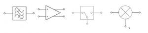
We call these Intelligent Gain blocks. From our mission perspective, Anokiwave’s mission is – how can we commercialize phased arrays be it for 5G, SATCOM, Aerospace & Defense, or RADAR. Our initial products were the quad core ICs for Active Antennas, but as we start to think about system level design, there are many elements to consider – and this is where the single channel block comes into play. In a traditional RF signal chain, you see gain degradation and power degradation and gain blocks are used to compensate for the losses. In arrays, the same issues occur, but now phase degradation is added. So that was the main driver in developing these integrated ICs that have gain and phase adjustment that can be used across the array to compensate for gain as well as phase. As we started developing these parts, we realized that we have reached a maturity level with the silicon technology that we can meet or exceed the performance of discrete RF blocks designed with III/V technologies. For example, the IGB LNA has 1.5 dB of noise figure in Ku-band – almost equal to performance to GaAs LNAs – technically, a GaAs LNA can be replaced with an integrated block like this.
As we introduce these parts, we see multiple use cases, the main driver being allowing for the compensation across the arrays, but now these parts are being considered for discrete RF functions – LNA, driver amplifier, phase or vector modulator, or VGA.
Finally, we recognize that in the 5G market, there is not going to be just one type of architecture. Anokiwave recommends an all silicon, quad approach, but as addressed in the February 2018 issue, there are companies promoting the column fed architecture with multiple transmit/receive paths feeding into a single column – the single channel ICs can integrate into the entire transmit and receive path – i.e. for 10 columns, 10 ICs can be used to provide the required gain and phase control on each column, thus simplifying the design. We expect the market will be impressed with the performance of these ICs.

4. What is Anokiwave featuring at IMS in Philadelphia?

5G is no longer a concept, but a reality. The waiting game is over. We have 2nd generation solutions covering all the bands of interest – 24/26, 28, and 37/39 GHz. Similarly, we have solutions for SATCOM, X-Band RADAR, and A/D markets. Across the board, if a customer is working on a flat panel array for these applications, Anokiwave has a solution today. The market is ready, we are ready with many products and options from which to select. A new product announcement we would like to make here on this show is the availability of the second set of ICs in the Intelligent Gain Block™ family. Two parts, one covering Ku-band and the other for Ka-band without the input T/R switch resulting in a single silicon IC that includes a PA, LNA, gain and phase control for both the transmit and receive paths with more flexibility in use of the ICs. –by Abhishek Kapoor

Mark Hoffman No Comments

What makes for a perfect Low Noise Amplifier (LNA) MMIC for your microwave system? The answer could be right under your noise figure.

Low Noise Amplifiers (LNAs) are a critical component in virtually all radar, wireless communications and instrumentation systems. But while the noise figure (NF) performance is often your primary focus, other microwave system considerations related to performance and size, weight, power and cost (SWaP-C) can be equally, if not more important. In this blog we’ll describe a few other key characteristics that may help you save time during your design cycle, save money during assembly, and even enhance your microwave assembly or subsystem at-large.

1. Input Power Survivability
Specifically in military and aerospace radar and communications applications, where electronic countermeasures (ECMs) may be used to overwhelm a receiver, a receiver must be capable of withstanding high levels of input power for varying intervals of time. Active or passive jamming can cause levels of noise and frequency bursts that couple large amounts of broadband or frequency-selective interference into a receiver. Moreover, in these applications there is often a high-power transmitter in close proximity to the receiver, which can lead to substantial coupling and power ingress into the receiver front end.

A common method to reduce the impact of critically high input powers to a receiver is to include a limiter or circulator on the input of a receiver chain. An unfortunate side effect of adding anything prior to the LNA in the receiver is the degradation of the overall system noise figure. These signal chain additions reduce the sensitivity of the receiver, which may shorten communications range, throughput, radar range and accuracy, and cause delays in acquiring mission critical information. A great 1 dB system noise figure can effectively become 2 dB or more when adding protection circuitry.

It’s thus very important to consider an LNA’s highest input power handling (or input survivability). Most LNAs can handle only 10-15 dBm pulsed on their input, but the highest achievers are now surviving 20 dBm continuously and 23-25 dBm pulsed and can help you eliminate the protection circuitry.

2. Gain Flatness, and Gain Stability over Temperature
Gain flatness across your required band is essential to achieve required inter-symbol-interference (ISI) levels and optimal range performance. As costly equalizers are often employed to compensate for the downward gain slope of typical LNAs, positive gain slope LNAs reduce that need.

Another factor to consider is gain stability over temperature. In applications such as aerospace communications, and SatCom, operating temperature can exceed 180 degrees F of variation within a short time window.

Temperature changes that are significant can affect an LNA by more than just changing the noise figure of the device and system; they can vary the frequency-dependent gain of the LNA. For example, large-phased array antennas may have thousands of TR modules, with many of the modules exposed to a variety of temperature gradients. If the communications system relies on gain stability throughout the TR modules, and the LNAs gain stability is temperature dependent, the system may suffer a significant loss in performance.

3. Supply Voltage and Power Consumption
Properly biasing a MMIC amplifier is critical to achieving adequate device performance. Depending upon the particular LNA design, the biasing circuitry could be composed of a positive and negative biasing circuit with temperature compensation. Some LNA MMICs have the biasing and compensation circuitry built in, but a positive and negative voltage supply must be provided to the exact specification for the biasing network to operate properly.

When designing at a system-level for a large RF or microwave assembly, many different voltage supplies may be required. Certain design constraints may also limit the noise and stability performance of those power supplies, which may impact the practical LNA performance due to limited power supply rejection ratio (PSRR). To avoid this, additional circuitry may be used to condition the voltage supplies for a given LNA MMIC. Each of these circuits and connection points introduces a potential failure mode to the voltage supplies, and thus impacts system reliability. These supply-voltage circuits also consume valuable assembly real estate and power, contribute to the overall size/weight of the assembly, add costs, and of course, consume design and test time.

In order to reduce the infrastructure necessary to integrate a MMIC LNA into a microwave assembly, engineers at Custom MMIC have applied innovative circuit-design techniques. The designs they have implemented, which only require a single positive voltage supply, also enable a wide range of voltage input for even greater flexibility. All of the necessary circuitry to properly bias these LNAs is integrated into the MMIC itself. Ultimately, when your MMIC requires only a single positive supply voltage it reduces your bill-of-material, overall system complexity, failure modes, and overall system SWaP-C.

In mobile platforms, including aerospace and satellite communications, power constraints are also a system-wide limitation that often dictates what solutions can be used. Moreover, for these applications, the power requirements of the components directly lead to the overall size and cost of the power generation circuits, and hence, the total system SWAP-C. An example of this concept is seen with satellite communications. The power required by a phased-array antenna must be generated by solar cells mounted on the satellite, which is one of the largest contributing factors of satellite weight and size. As launching satellites costs thousands to tens of thousands of dollars per kilogram, reducing the weight of a satellite system can directly influence the cost-per-bit of high-speed satellite communication services.

If your next LNA might find itself in a similar system, be sure its power consumption (bias current and bias voltage) is as efficient as possible. LNAs with lower power needs are also typically smaller, demonstrate better temperature performance, and provide better SNR at lower power levels. –Blog by Custom MMIC

Mark Hoffman No Comments

Breakthrough Ultra Low Noise Amplifier Has 0.6 dB Noise Figure and Covers 2-6 GHz Frequency Range

Breakthrough Ultra Low Noise Amplifier Has 0.6 dB Noise Figure and Covers 2-6 GHz Frequency Range
We’re proud to announce that we’ve recently released a new GaAs Low Noise Amplifier (LNA) MMIC with broadband noise figure performance previously only achievable with discrete FET designs. The CMD283C3, with 0.6dB noise figure, is the first in a family of new Ultra Low Noise Amplifiers.

The CMD283C3 LNA covers 2-6 GHz with high midband gain of 27 dB and output P1dB of 16dBm. The MMIC is housed in a leadless 3×3 mm surface mount package. It operates from a bias supply of +2 to +5 volts and draws a nominal 42mA. The CMD283C3 is ideally suited for S and C band receivers requiring excellent sensitivity, and as a replacement for discrete FET LNA solutions.

Visit https://www.custommmic.com/cmd283c3/for more information and to download full datasheet and S-parameter data. – Custom MMIC

Mark Hoffman No Comments

Give your Applications a boost with Leader Tech Thermal Solutions

Leader Tech has launched a wide array of high-quality thermal solutions that are capable of withstanding extreme temperature and meeting the stringent industry standards. The products are crafted with utmost care to meet the needs of the clients and provide efficient performance. From thermal gap fillers to insulators, graphite thermal gaskets to thermal tapes, Leader Tech has ensured that something for every type of thermal application is easily made available to consumers. -Read entire blog at Leader Tech Inc.

Mark Hoffman No Comments

Selecting a Power Sensor by LadyBug Tech Products

True RMS Sensors 9 kHz to 40 GHz
HIGH ACCURACY ON ANY SIGNAL WITH ANY MODULATION

LadyBug True RMS Average Power Sensors deliver reliable, accurate power measurements for CW, Pulse, and modulated signals. These diode based sensors feature a wide dynamic range and a great VSWR. The optional external triggering input feature can be used without any external components. Recorder and Trigger outputs are also available. Our patented NoZero NoCal technology make these sensors ideal for calibration systems, automated test stations and other embedded applications.

Peak, Pulse and Averaging Sensors 10 MHz to 20 GHz
STATISTICAL PULSE & FAST AVERAGE MEASUREMENTS

These sensors provide quick and easy measurements of pulse power, continuous wave power and other signals. Many of our competitors claim to measure pulse power, however you must input your duty cycle and the power is calculated based on that. Our sensors offer trigger based measurements and the pulse itself is examined giving better measurement uncertainty. There is no need to input the duty cycle to calculate pulse measurements, our sensors measure it.

Wideband Pulse Profiling Sensors 50 MHz to 20 GHz
VISUAL TIME DOMAIN PULSE PROFILE, PULSE & FAST AVERAGE MEASUREMENTS

LadyBug wideband Power Sensors feed power waveform samples into high speed A/D converters. The measured power is processed and then delivered as required by the user. These sensors are capable of delivering everything from basic power, to time domain scope-like profiles of the modulated waveform, such as the pulse shown at right. Multiple time gated measurements, crest factor, pulse power, and statistical measurements are all possible with these sensors.

Learn more at LadyBug Tech Products