The Gallium Nitride (GaN) high electron mobility transistor (HEMT) is well known for its use in microwave and millimeter wave power amplifiers due to its high breakdown voltage and ability to handle high RF power. Recently, GaN technology has also been used to create low noise amplifiers (LNAs) in the microwave region, as the noise properties of GaN are similar to other semiconductor materials, most notably Gallium Arsenide (GaAs). In many microwave systems, LNAs are subject to unwanted high input power levels such as jamming signals. One of the features of LNAs made from GaN is the ability to withstand these input power levels without the need for a limiter, due to the inherent robustness of the device. Indeed, this is one reason GaN LNAs are supplanting their GaAs counterparts, since GaAs LNAs typically require a front-end limiter, which adds to the cost and degrades the performance of the LNA.
Despite the ability to operate without a limiter, GaN LNAs, however, are not completely immune to the effects of high input power. The problem occurs when both a high power jamming signal and the desired signal are input to the GaN LNA, and then the jamming signal is suddenly turned off. Under this scenario, the GaN amplifier does not recover immediately, as there is some residual distortion of the desired signal before normal operation returns. This phenomenon is known as pulse recovery time and is fast becoming an important parameter with regards to LNAs in general. Past researchers have studied pulse recovery times in GaN LNAs, although this work has been limited in scope. One study presented recovery times of less than 30 ns in some amplifiers, but these measurements only utilized a coherent jammer, and the overall number of measurements was limited. A second investigation of pulse recovery time was performed on a GaAs LNA with a limiter. The limiter not only effected the small signal performance, but it also increased the recovery time when high power was applied. Further research has been performed on the degradation of GaN HEMT noise performance after exhibiting DC and RF stress, which can cause forward gate current and damage the gate device. However, this work did not explicitly address pulse recovery times in LNAs. Other papers have similarly analyzed the survivability of GaN amplifiers to high input power overdrive, but again this work offers little understanding of pulse recovery times.
MEASUREMENT TEST SETUP
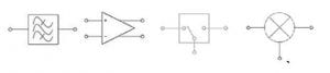
A setup designed by Custom MMIC uses two signal generators, where the first provides the out-of-band interfering signal at 8.5 GHz, and the second provides the desired continuous wave (CW) in-band signal at 7.5 GHz. The interfering RF signal from #1 is pulsed using a single pole single throw (SPST) switch controlled by a square wave with a low duty cycle. We chose to pulse the signal path, as opposed to the bias circuitry of the interferer amplifier, due to the fast rise/fall time of the SPST, which is on the order of 1.8 ns. Additionally, pulsing the power supply caused high levels of ringing to appear at the output. The interfering signal was amplified by an external power amplifier (PA) and then added to the desired signal with a passive power combiner. We utilized a circulator, terminated in a 20 dB pad and a high power 50 Ohm load, between the combiner and the device under test (DUT) in order to prevent any high power mismatch signal from reflecting back into the PA. The output of the DUT was then attenuated with an additional 20 dB pad, sent through a band pass filter with a pass band of 7.25 to 7.75 GHz, and then input into a digitizing oscilloscope. The filter attenuates the interfering signal to allow for an accurate measurement of the pulse recovery time. Finally, we utilized two different oscilloscopes for the measurement. A Tektronix digital serial analyzer oscilloscope was used to measure the recovery time for the shorter pulse widths, while a Hewlett Packard Digitizing Oscilloscope was used to measure the recovery time when longer pulses were used.
The test procedure consisted of varying the pulse width and the input power of the interfering signal, while keeping the power of the desired signal constant at -10 dBm. A summary of the test conditions including pulse widths, repetition rates, and power levels of the interfering signal are presented in our tech brief . Notably, the input power of the interfering signal was varied between 15 and 27 dBm, with the total energy delivered to the DUT being the important parameter of concern. All measurements with short pulses were performed on the Tektronix oscilloscope, whereas the long pulse measurements were performed on the Hewlett-Packard oscilloscope.
Blog by Custom MMic
Learn more about the study of pulse recovery times in GaN LNA’s.