Mark Hoffman No Comments

How to Ensure Corrosion Resistant EMI Protection

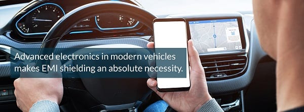
EMI shielding products are designed to protect electronics from the effects of interfering energy waves. But what happens when you use your equipment in an extremely damp environment? In such a situation, your priority should be to make your EMI shielding products corrosion-resistant. Rust or material deterioration will affect device performance due to high-frequency emissions interfering with your electronic gadgets. Here are a few ways to protect your equipment from corrosion:

Consider Surface Treatment

Paint or plate your electronic enclosures. It is essential to prevent corrosion, oxidation, rusting, and tarnishing. Maintain application aesthetics. When it comes to the flange surfaces, they require finishing for maximum protection against corrosion. There are a few factors to consider when employing finishing. You must ensure maximum shielding efficiency through corrosion-resistant and electrically conductive materials. You will require an additional coating for protecting shielded products from being corroded in high humidity surroundings.

Pick out Quality EMI Gaskets

Choose the right gasket material that can cut back the variation in electrochemical potential in relation to the metal structure. It helps to decelerate the corrosion process through a lower galvanic current. Opt for elastomeric gaskets that come with filler particles. The material will ensure both corrosion resistance and EMI shielding when exposed to metal. Use silver-plated copper, pure silver, and silver-plated aluminum fillers to ensure corrosion resistant EMI protection.

Opt for Additional Moisture Sealing

Spray or salt fog acting as an electrolyte may corrode your shielding materials. This is the reason why designers require secondary moisture sealing to get rid of it. To prevent corrosion in aircraft applications, a seal-to-seal design is the preferred choice of EMI shielding engineers. Similar gasket materials are used in every mating flange. Non-conductive sealers are used to stop water from seeping into your shielded products.

Choose the right EMI gasket material for protection against water, fog, or salt spray. The use of conductive coating and an additional moisture seal will keep corrosion under control for improved shielding effectiveness. If you want to learn more about our products, contact us today. -LeaderTechInc.com

Mark Hoffman No Comments

pSemi Releases World’s First, Fully Integrated, 8-channel LED Boost

Power Supply in Package (PSiP) Uses a Unique Design Based on a Patented, Two-stage Architecture that Relies on Capacitors to Handle the Bulk of the Power-conversion Work

SAN ANTONIO – APPLIED POWER ELECTRONICS CONFERENCE (APEC) – March 6, 2018 – pSemi Corporation (formerly Peregrine Semiconductor), a Murata company focused on semiconductor integration, introduces the PE23300, the industry’s only fully integrated LED boost power supply in package (PSiP) based on a charge-pump, switched-capacitor architecture that offloads most of the power-conversion work from the inductor to capacitors in the charge pump.

Powering up to eight LED strings at a total power level of up to 10 watts, the PE23300 is designed specifically to power LED backlight arrays in ultra-high-definition (UHD) and high definition (HD) LCD panels for 2-cell and 3-cell narrow-voltage DC notebooks, industrial and automotive displays.

PE23300 Fully Integrated 8-channel LED Boost

“The PE23300 truly demonstrates pSemi’s power-semiconductor capabilities. The PSiP delivers a unique, two-stage architecture that brings ground-breaking conversion efficiency and small solution size and is packaged with Murata’s advanced, 3D-packaging technology and passive components,” says Stephen Allen, director of strategic marketing at pSemi. “All components required for operation are integrated into a 7.7 x 11.7 millimeter laminate-based LGA package, which is just 1.6 millimeters in height. To achieve this small size, we used a ‘die-in-substrate’ 3D-packaging technology. The low profile is also a result of our two-stage architecture that allows us to use a tiny chip inductor. All of this can be achieved with an efficiency that is on average about 5 to 7 percent higher than the competition, halving the losses in the LED boost.”

Power conversion creates a compromise between size and efficiency: The smaller the solution, the worse the efficiency. This compromise impacts OEMs trying to make next-generation, ultra-compact products, because they need both a very high conversion efficiency and a very small size at the same time. pSemi solves this problem with a novel, two-stage architecture that offloads most of the power-conversion work from the inductor to a virtually lossless charge pump and relies on small, multilayer ceramic capacitors (MLCCs) to do most of the work. As a result, the inductor – usually the largest and tallest component – can be reduced dramatically in size, and traditional wire-wound inductors can be replaced with chip inductors. This patented architecture was first developed by Arctic Sand Technologies, an MIT spin-out acquired by pSemi in March 2017, and commercialized this year.

Beyond the smaller inductor and higher efficiency, this architecture delivers several other key benefits for LED boosts, including full short-circuit protection and a very flat efficiency over the entire load range. Also, efficiency is virtually independent of the output voltage, and this allows more LEDs per string. With fewer strings, efficiency is optimized, and the display-bezel size can be reduced in width. pSemi’s PE23300 features low power dissipation – up to half that of competing products – that improves reliability and supports portable applications’ extensive battery run times.

Product Features

The PE23300 features an input voltage range of 4.5V to 15V DC and powers up to eight strings of LEDs at up to 45V and 40 mA per string.

The PSiP provides full programmability via an I2C interface with settings stored in non-volatile memory or by using GPR pins. Dimming resolution is up to 12-bits resolution with an additional 3-bit dithering and can be either linear/logarithmic analog and PWM dimming or direct PWM dimming for maximum flexibility and resolution. The part features an LED brightness ramp up/down control with programmable ramp rate, linear/logarithmic ramp profiles and phase-shifted PWM dimming among active strings to minimize audible noise.

About pSemi 

pSemi Corporation is a Murata company driving semiconductor integration. pSemi builds on Peregrine Semiconductor’s 30-year legacy of technology advancements and strong IP portfolio but with a new mission: to enhance Murata’s world-class capabilities with high-performance RF, analog, mixed-signal and optical solutions. With a strong foundation in RF integration, pSemi’s product portfolio now spans power management, connected sensors, optical transceivers antenna tuning and RF frontends. These intelligent and efficient semiconductors enable advanced modules for smartphones, base stations, personal computers, electric vehicles, data centers, IoT devices and healthcare. From headquarters in San Diego and offices around the world, pSemi’s team explores new ways to make electronics for the connected world smaller, thinner, faster and better. To view pSemi’s semiconductor advancements or to join the pSemi team, visit www.psemi.com.

###

The Peregrine Semiconductor name, Peregrine Semiconductor logo and UltraCMOS are registered trademarks and the pSemi name, pSemi logo, HaRP and DuNE are trademarks of pSemi Corporation in the U.S. and other countries. All other trademarks are the property of their respective companies. The pSemi website is copyrighted by pSemi Corporation. All rights reserved.

Mark Hoffman No Comments

Is It True That Today’s Auto-Makers Rely Heavily on the EMI-Shielding Industry?

Rapid advancements in electromagnetic interference (EMI) shielding technology has served to make the driving experience in modern vehicles smooth and hassle-free. The addition of new systems, such as on-board GPS, in-vehicle communication, wireless charging, and touchscreen infotainment, is a big draw for modern consumers and increases the value of a vehicle considerably. Unfortunately, these devices are also responsible for the emission of unwanted EMI. The problem is compounded by the constant use of smartphones, tablets, and other wireless equipment in and around cars. While these emissions pose a threat to automobile applications, they create opportunities for shielding materials to grow in this sector.

More EMI in Vehicles Means More Shielding

EMI emission varies across automobile technologies, and so does the need for EMI shielding. For example, protection is a must in cars employing advanced electronics for engine performance. Still, automobile manufacturers need to get in touch with EMI shielding suppliers and implement the technology early on during the design stages. That’s because, the more personalized and innovative the solution, the better.

Electric motors and other electronic systems appear to be the most culpable among all automobile technology. They emit massive levels of EMI that cause widespread problems, ranging from malfunctions to breakdowns. So, for the protection of the different components in vehicles and ensuring they are compatible, modern car designers should make provisions for EMI shielding.

Relation Between Automobile Manufacturing Materials and EMI

The evolving nature of the materials used to construct modern vehicles means EMI shielding must keep up at all times. New vehicles utilize sheet metal to deter external EMI. With more and more automobile companies switching to non-metallic components for the production of auto body parts, it might be a good idea for shielding engineers to redirect their efforts towards devising a foolproof solution for the protection of the vehicle interiors.

Hurdles in Store

The process of designing EMI shielding for a new vehicle model is time-consuming and expensive, but it should not be neglected. Detection of EMI issues late in production can bring the manufacturing process to a halt while the engineers attempt to uncover what went wrong. Perhaps the biggest hurdle lies in figuring out the perfect moment to install shielding in vehicles. Often, EMI signals, like those produced in vehicle interiors, are so faint that it is difficult to figure out which components are at risk. But implementing EMI shielding during the design process increases its effectiveness while decreasing the cost.

The growing demand for integrated electronics within vehicles means the EMI shielding industry will need to step up its game.  There will be hurdles, of course, but with the right design, materials, and manufacturing process, successful EMI shielding can be a reality. To know more about vehicular EMI shielding, contact us here. – Blog by Leader Tech

Mark Hoffman No Comments

Kratos’ Microwave Electronics: Switches/Attenuators

Kratos’ General Microwave offers a wide range of microwave attenuators both as COTS and as customized products.

Main Features:

  • Digitally, Voltage and Current Controlled
  • Switch Bit Attenuators
  • Broad Frequency Bands
  • Monotonicity
  • High Linearity
  • Phase Invariant Attenuators
  • Low Resolution

**

For the past 50 years, Kratos’ General Microwave has been an industry standard in microwave discrete pin diode switches. Today, Kratos’ General Microwave’s catalog line of switches offers the designer a cost effective approach for discrete components needs by offering a comprehensive catalog of SPST to SP16T switches, with various standard options as COTS products. In addition, Kratos’ General Microwave offers customized switches.

Main Features:

  • Operating Frequencies from .1 – 40 GHz
  • Reflective and Non-Reflective
  • Fast Switching Time
  • High Isolation
  • Phase and Amplitude Matched (between ports)
  • Low Video Leakage
  • Driver and Driverless Switches

Kratos’ General Microwave’s catalog line of switches includes:

**
For over 50 years, Kratos’ General Microwave has been a leading supplier of RF/microwave and millimeter wave products and technology solutions. Primarily focused on electronic warfare, ECM and radar applications, Kratos’ General Microwave supplies a comprehensive portfolio of COTS products, as well as highly complex, highly integrated assemblies and sub-systems.

Our manufacturing facility incorporates state-of-the-art design simulation capabilities, state-of-the-art automated testing and phase noise measurement equipment. Many of the most stringent environmental tests are conducted in-house due to our extensive environmental test capability.

To date, we have delivered thousands of integrated assemblies and systems for military applications, with most of these having been proven successful in a combat environment.

For more information about Kratos’ General Microwave’s Integrated Microwave Assemblies products.

Mark Hoffman No Comments

The Study of Pulse Recovery Times in GaN LNAs: Part I

The Gallium Nitride (GaN) high electron mobility transistor (HEMT) is well known for its use in microwave and millimeter wave power amplifiers due to its high breakdown voltage and ability to handle high RF power. Recently, GaN technology has also been used to create low noise amplifiers (LNAs) in the microwave region, as the noise properties of GaN are similar to other semiconductor materials, most notably Gallium Arsenide (GaAs). In many microwave systems, LNAs are subject to unwanted high input power levels such as jamming signals. One of the features of LNAs made from GaN is the ability to withstand these input power levels without the need for a limiter, due to the inherent robustness of the device. Indeed, this is one reason GaN LNAs are supplanting their GaAs counterparts, since GaAs LNAs typically require a front-end limiter, which adds to the cost and degrades the performance of the LNA.

Despite the ability to operate without a limiter, GaN LNAs, however, are not completely immune to the effects of high input power. The problem occurs when both a high power jamming signal and the desired signal are input to the GaN LNA, and then the jamming signal is suddenly turned off. Under this scenario, the GaN amplifier does not recover immediately, as there is some residual distortion of the desired signal before normal operation returns. This phenomenon is known as pulse recovery time and is fast becoming an important parameter with regards to LNAs in general. Past researchers have studied pulse recovery times in GaN LNAs, although this work has been limited in scope. One study presented recovery times of less than 30 ns in some amplifiers, but these measurements only utilized a coherent jammer, and the overall number of measurements was limited. A second investigation of pulse recovery time was performed on a GaAs LNA with a limiter. The limiter not only effected the small signal performance, but it also increased the recovery time when high power was applied. Further research has been performed on the degradation of GaN HEMT noise performance after exhibiting DC and RF stress, which can cause forward gate current and damage the gate device. However, this work did not explicitly address pulse recovery times in LNAs. Other papers have similarly analyzed the survivability of GaN amplifiers to high input power overdrive, but again this work offers little understanding of pulse recovery times.

MEASUREMENT TEST SETUP

A setup designed by Custom MMIC uses two signal generators, where the first provides the out-of-band interfering signal at 8.5 GHz, and the second provides the desired continuous wave (CW) in-band signal at 7.5 GHz. The interfering RF signal from #1 is pulsed using a single pole single throw (SPST) switch controlled by a square wave with a low duty cycle. We chose to pulse the signal path, as opposed to the bias circuitry of the interferer amplifier, due to the fast rise/fall time of the SPST, which is on the order of 1.8 ns. Additionally, pulsing the power supply caused high levels of ringing to appear at the output. The interfering signal was amplified by an external power amplifier (PA) and then added to the desired signal with a passive power combiner. We utilized a circulator, terminated in a 20 dB pad and a high power 50 Ohm load, between the combiner and the device under test (DUT) in order to prevent any high power mismatch signal from reflecting back into the PA. The output of the DUT was then attenuated with an additional 20 dB pad, sent through a band pass filter with a pass band of 7.25 to 7.75 GHz, and then input into a digitizing oscilloscope. The filter attenuates the interfering signal to allow for an accurate measurement of the pulse recovery time. Finally, we utilized two different oscilloscopes for the measurement. A Tektronix digital serial analyzer oscilloscope was used to measure the recovery time for the shorter pulse widths, while a Hewlett Packard Digitizing Oscilloscope was used to measure the recovery time when longer pulses were used.

The test procedure consisted of varying the pulse width and the input power of the interfering signal, while keeping the power of the desired signal constant at -10 dBm. A summary of the test conditions including pulse widths, repetition rates, and power levels of the interfering signal are presented in our tech brief . Notably, the input power of the interfering signal was varied between 15 and 27 dBm, with the total energy delivered to the DUT being the important parameter of concern. All measurements with short pulses were performed on the Tektronix oscilloscope, whereas the long pulse measurements were performed on the Hewlett-Packard oscilloscope.

Blog by Custom MMic

Learn more about the study of pulse recovery times in GaN LNA’s.