Mark Hoffman No Comments

Is It True That Today’s Auto-Makers Rely Heavily on the EMI-Shielding Industry?

Rapid advancements in electromagnetic interference (EMI) shielding technology has served to make the driving experience in modern vehicles smooth and hassle-free. The addition of new systems, such as on-board GPS, in-vehicle communication, wireless charging, and touchscreen infotainment, is a big draw for modern consumers and increases the value of a vehicle considerably. Unfortunately, these devices are also responsible for the emission of unwanted EMI. The problem is compounded by the constant use of smartphones, tablets, and other wireless equipment in and around cars. While these emissions pose a threat to automobile applications, they create opportunities for shielding materials to grow in this sector.

More EMI in Vehicles Means More Shielding

EMI emission varies across automobile technologies, and so does the need for EMI shielding. For example, protection is a must in cars employing advanced electronics for engine performance. Still, automobile manufacturers need to get in touch with EMI shielding suppliers and implement the technology early on during the design stages. That’s because, the more personalized and innovative the solution, the better.

Electric motors and other electronic systems appear to be the most culpable among all automobile technology. They emit massive levels of EMI that cause widespread problems, ranging from malfunctions to breakdowns. So, for the protection of the different components in vehicles and ensuring they are compatible, modern car designers should make provisions for EMI shielding.

Relation Between Automobile Manufacturing Materials and EMI

The evolving nature of the materials used to construct modern vehicles means EMI shielding must keep up at all times. New vehicles utilize sheet metal to deter external EMI. With more and more automobile companies switching to non-metallic components for the production of auto body parts, it might be a good idea for shielding engineers to redirect their efforts towards devising a foolproof solution for the protection of the vehicle interiors.

Hurdles in Store

The process of designing EMI shielding for a new vehicle model is time-consuming and expensive, but it should not be neglected. Detection of EMI issues late in production can bring the manufacturing process to a halt while the engineers attempt to uncover what went wrong. Perhaps the biggest hurdle lies in figuring out the perfect moment to install shielding in vehicles. Often, EMI signals, like those produced in vehicle interiors, are so faint that it is difficult to figure out which components are at risk. But implementing EMI shielding during the design process increases its effectiveness while decreasing the cost.

The growing demand for integrated electronics within vehicles means the EMI shielding industry will need to step up its game.  There will be hurdles, of course, but with the right design, materials, and manufacturing process, successful EMI shielding can be a reality. To know more about vehicular EMI shielding, contact us here. – Blog by Leader Tech

Mark Hoffman No Comments

Kratos’ Microwave Electronics: Switches/Attenuators

Kratos’ General Microwave offers a wide range of microwave attenuators both as COTS and as customized products.

Main Features:

  • Digitally, Voltage and Current Controlled
  • Switch Bit Attenuators
  • Broad Frequency Bands
  • Monotonicity
  • High Linearity
  • Phase Invariant Attenuators
  • Low Resolution

**

For the past 50 years, Kratos’ General Microwave has been an industry standard in microwave discrete pin diode switches. Today, Kratos’ General Microwave’s catalog line of switches offers the designer a cost effective approach for discrete components needs by offering a comprehensive catalog of SPST to SP16T switches, with various standard options as COTS products. In addition, Kratos’ General Microwave offers customized switches.

Main Features:

  • Operating Frequencies from .1 – 40 GHz
  • Reflective and Non-Reflective
  • Fast Switching Time
  • High Isolation
  • Phase and Amplitude Matched (between ports)
  • Low Video Leakage
  • Driver and Driverless Switches

Kratos’ General Microwave’s catalog line of switches includes:

**
For over 50 years, Kratos’ General Microwave has been a leading supplier of RF/microwave and millimeter wave products and technology solutions. Primarily focused on electronic warfare, ECM and radar applications, Kratos’ General Microwave supplies a comprehensive portfolio of COTS products, as well as highly complex, highly integrated assemblies and sub-systems.

Our manufacturing facility incorporates state-of-the-art design simulation capabilities, state-of-the-art automated testing and phase noise measurement equipment. Many of the most stringent environmental tests are conducted in-house due to our extensive environmental test capability.

To date, we have delivered thousands of integrated assemblies and systems for military applications, with most of these having been proven successful in a combat environment.

For more information about Kratos’ General Microwave’s Integrated Microwave Assemblies products.

Mark Hoffman No Comments

The Study of Pulse Recovery Times in GaN LNAs: Part I

The Gallium Nitride (GaN) high electron mobility transistor (HEMT) is well known for its use in microwave and millimeter wave power amplifiers due to its high breakdown voltage and ability to handle high RF power. Recently, GaN technology has also been used to create low noise amplifiers (LNAs) in the microwave region, as the noise properties of GaN are similar to other semiconductor materials, most notably Gallium Arsenide (GaAs). In many microwave systems, LNAs are subject to unwanted high input power levels such as jamming signals. One of the features of LNAs made from GaN is the ability to withstand these input power levels without the need for a limiter, due to the inherent robustness of the device. Indeed, this is one reason GaN LNAs are supplanting their GaAs counterparts, since GaAs LNAs typically require a front-end limiter, which adds to the cost and degrades the performance of the LNA.

Despite the ability to operate without a limiter, GaN LNAs, however, are not completely immune to the effects of high input power. The problem occurs when both a high power jamming signal and the desired signal are input to the GaN LNA, and then the jamming signal is suddenly turned off. Under this scenario, the GaN amplifier does not recover immediately, as there is some residual distortion of the desired signal before normal operation returns. This phenomenon is known as pulse recovery time and is fast becoming an important parameter with regards to LNAs in general. Past researchers have studied pulse recovery times in GaN LNAs, although this work has been limited in scope. One study presented recovery times of less than 30 ns in some amplifiers, but these measurements only utilized a coherent jammer, and the overall number of measurements was limited. A second investigation of pulse recovery time was performed on a GaAs LNA with a limiter. The limiter not only effected the small signal performance, but it also increased the recovery time when high power was applied. Further research has been performed on the degradation of GaN HEMT noise performance after exhibiting DC and RF stress, which can cause forward gate current and damage the gate device. However, this work did not explicitly address pulse recovery times in LNAs. Other papers have similarly analyzed the survivability of GaN amplifiers to high input power overdrive, but again this work offers little understanding of pulse recovery times.

MEASUREMENT TEST SETUP

A setup designed by Custom MMIC uses two signal generators, where the first provides the out-of-band interfering signal at 8.5 GHz, and the second provides the desired continuous wave (CW) in-band signal at 7.5 GHz. The interfering RF signal from #1 is pulsed using a single pole single throw (SPST) switch controlled by a square wave with a low duty cycle. We chose to pulse the signal path, as opposed to the bias circuitry of the interferer amplifier, due to the fast rise/fall time of the SPST, which is on the order of 1.8 ns. Additionally, pulsing the power supply caused high levels of ringing to appear at the output. The interfering signal was amplified by an external power amplifier (PA) and then added to the desired signal with a passive power combiner. We utilized a circulator, terminated in a 20 dB pad and a high power 50 Ohm load, between the combiner and the device under test (DUT) in order to prevent any high power mismatch signal from reflecting back into the PA. The output of the DUT was then attenuated with an additional 20 dB pad, sent through a band pass filter with a pass band of 7.25 to 7.75 GHz, and then input into a digitizing oscilloscope. The filter attenuates the interfering signal to allow for an accurate measurement of the pulse recovery time. Finally, we utilized two different oscilloscopes for the measurement. A Tektronix digital serial analyzer oscilloscope was used to measure the recovery time for the shorter pulse widths, while a Hewlett Packard Digitizing Oscilloscope was used to measure the recovery time when longer pulses were used.

The test procedure consisted of varying the pulse width and the input power of the interfering signal, while keeping the power of the desired signal constant at -10 dBm. A summary of the test conditions including pulse widths, repetition rates, and power levels of the interfering signal are presented in our tech brief . Notably, the input power of the interfering signal was varied between 15 and 27 dBm, with the total energy delivered to the DUT being the important parameter of concern. All measurements with short pulses were performed on the Tektronix oscilloscope, whereas the long pulse measurements were performed on the Hewlett-Packard oscilloscope.

Blog by Custom MMic

Learn more about the study of pulse recovery times in GaN LNA’s.

Mark Hoffman No Comments

Advanced MMICs Aid in Reducing Size and Power in Phased Array Radar Systems

Phased-array radar systems are important instruments in national electronic defense strategies. From the large, ship-based systems that scan for distantly launched missiles to the more compact arrays installed on fighter aircraft and unmanned aerial vehicles (UAVs), electronic phased-array radars come in many sizes and forms, providing reliable signal detection and identification. These modern systems offer many advantages over earlier radar systems that relied on the physical movement of an antenna to steer a radar beam in search of a target. This earlier method is certainly proven and reliable, having been used in military platforms and commercial aviation for over 70 years, but it is limited in scan rate by the mechanical motion of the antenna. In contrast, a phased-array radar system uses many equally spaced antenna elements with phase shifters, with each element contributing a small amount of electromagnetic (EM) radiation to form a much larger beam. As the phase of each antenna element is shifted and aligned, the direction of the radar beam changes and, as the amplitude of each element is varied, the pattern of the far-field response is shaped into the desired response. Thus, the overall radar antenna beam can be steered without need of a mechanically rotated antenna. Beam forming, which can be now performed by means of analog or digital control, can take place at extremely high speeds, limited only by the switching speed of electronic components

Historically, phased-array radar systems have been large in both cost and weight. With the explosive growth of UAVs and unmanned ground vehicles (UGVs) as key elements of the defense arsenal, the need for lighter phased-array radar systems in these weight-sensitive systems will continue to grow. In addition, the increased use of such radars for non-military applications, such as tornado detection by the US National Weather Service (Springfield, MO), is helping drive the demand for lower-cost systems. Fortunately, these growing demands placed on phased-array radar systems can be met with the help of modern RF/microwave integrated-circuit (IC) and monolithic-microwave-integrated-circuit (MMIC) technologies.

PHASED-ARRAY BENEFITS AND DRAWBACKS

The benefits of phased-array radar systems far outweigh their limitations, thus accounting for their growing use in many military electronic systems and platforms. Since beam steering in phased arrays can be performed at millisecond and faster speeds, the signal can jump from one target to the next very quickly, while frequency agility can be used to search quickly across a sector for targets. The coverage of a phased-array antenna beam is typically limited to a 120-deg. sector in azimuth and elevation. While this response is a known limitation of phased arrays, mechanically scanned radar systems also have limitations in the physical area available for the motion of the antenna. Important factors hindering the adoption of phased-array radar systems in many applications continue to be size, weight, power, and cost (SWAP-C). Efforts aimed at minimizing these four attributes represent a significant technological challenge that until recently has seemed a rather formidable hurdle. Phased array radars are, after all, quite complex and even growing in this regard as target identification becomes more difficult. How can SWAP-C reduction be accomplished?

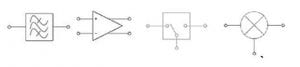
A phased-array radar system (Fig. 1) is constructed from large numbers (often thousands) of transmit/receive (T/R) modules which enable the array to function as both a transmitter and a receiver. Initially designed with discrete hybrid components such as amplifiers, filter, mixers, phase shifters, and switches, these modules are now more commonly fabricated with high-frequency IC or MMIC technology. This switchover to IC technology has provided tremendous benefits in terms of SWAP-C reduction, but simply replacing components can only get a designer so far. Gaining additional SWaP-C benefits in any phased-array radar system also requires knowledge of how to best apply available IC and MMIC technologies to the system (Fig. 2). In fact, the key characteristics of size, weight, and power consumption in a phased-array radar system can usually be minimized by analyzing the design at the circuit, system, and technology levels.

Analysis at the technology level first involves a choice of semiconductor material. Modern commercial semiconductor foundries typically offer a number of different material technologies, but a choice among these is not always straightforward. Components in high-frequency T/R modules typically include high-power amplifiers (HPAs) for transmit purposes, low-noise amplifiers (LNAs) for receiving purposes, mixers and oscillators for signal translation (frequency upconversion and downconversion), and attenuators, filters, and switches for signal conditioning. Fabricating MMICs for all of these functions will likely require more than one semiconductor technology. For example, processes based on silicon-carbide (SiC) or gallium nitride (GaN) substrates will excel in higher-power portions of the system such as transmit functions, while processes using silicon-germanium (SiGe) or gallium-arsenide (GaAs) materials will exhibit lower noise for better performance in receiver functions.

Analysis at the system and circuit levels should be closely intertwined, as a system is only as good as the sum of its components. Unfortunately, the vast majority of IC and MMIC circuit suppliers do not give enough consideration to any specific system, opting instead to create generic components that can be used across wide reaching applications. Such an approach, while cost-effective in terms of IC and MMIC development, is not always optimal in reducing SWaP-C since these components cannot be easily customized for use in phased array systems.

Forward-thinking MMIC suppliers, such as Custom MMIC, have worked on approaches that combine technology, system, and circuit analysis to create components that resolve SWaP-C challenges in phased array systems. At the technology level, they have worked with nearly all of the world’s commercial III-V semiconductor foundries, and have intimate knowledge of some of the newest processes including optical pHEMT and high frequency GaN. At the system level, they have been engaged with numerous phased array designers and have heard first-hand how yesterday’s components are holding back development of next-generation low cost, low weight, high performance systems. At the circuit level, they have created an extensive intellectual property (IP) design library of components in both die and packaged form that are used as a starting point for advanced signal chain design and optimization.

As an example, one place where they have focused significant development is the transmit HPA, a common component required in almost every application. At microwave and millimeter-wave frequencies, the transmit amplifier is often fabricated from a depletion mode pHEMT process, a highly efficient and mature technology. However, depletion mode pHEMT is not without its drawbacks, most notably the need for negative gate voltage and a sequencing procedure to ensure the gate voltage is applied before the drain voltage, lest the FET device suffer irreparable harm. By their very nature, negative voltages and sequencing circuits for HPAs are expensive in terms of complexity, board space, and cost of the extra components. In phased arrays, especially ones with thousands of elements, such HPAs place enormous strain on the system as a whole and offer significant barriers to SWaP-C reduction. Therefore, as part of a Small Business Innovative Research grant (SBIR) from the U. S. Army, they attacked this problem for the transmit portion of an X-band phased array system. Rather than utilize depletion mode pHEMT, they turned to enhancement mode pHEMT for the HPA, a technology often relegated to other applications such as high-speed logic circuitry or switches. In enhancement mode, the pHEMT is normally off until a positive voltage is applied to the gate. Negative voltages are no longer required, nor are voltage sequencers, since either the control or the drain voltage can be applied first; the amplifier will not turn on until both are present. In the end, they were able to replace the existing depletion mode PA with an enhancement mode design that delivered 5 dB more gain, 1 dB more power, and 2 dB improved linearity, all while dissipating 25% less DC power. In terms of SWaP-C, the benefits of enhancement mode PAs are enormous, and offer a significant breakthrough for microwave system designers in general.

A second problem they considered was the receiver LNA in an X-band phased array system as part of a separate SBIR contract. Here, they also switched from a depletion mode to an enhancement mode process, thereby eliminating the negative voltages and sequencers of the existing solution. Their resulting design had 1 dB lower noise figure, 8 dB more gain, an eight-fold reduction in DC power, and half the unit cost of the existing depletion mode solution. However, they soon encountered an application that called for a pair of relatively well-matched LNAs, one for each of the two polarizations in the return signal. Starting with their enhancement mode LNA, they created a dual version on one MMIC die, thereby guaranteeing a matched pair. They also worked with their packaging vendor to develop a low cost rectangular QFN plastic package to best match the resulting die size. The end result was a “standard” product that was anything but ordinary, as it combined innovation at the circuit, system, and technological levels to deliver a component with significant impact on SWaP-C.

Moving forward, they are continuing to develop components for phased array radar systems and similarly challenged 5G wireless systems. Using other technologies such as high frequency GaN, and a combination of different semiconductor devices in multi-chip modules, they’re looking to help designers when digital control functions must be integrated with higher frequency functions.

“We’re learning more everyday about phased array radar and antenna system design challenges,“ says Custom MMIC CSO, Charles Trantanella. “Our product design approach has always been to listen and react, and we’re very pleased to have been able to not only deliver the high frequency performance specifications phased array system designers were looking for, but also the added-value of things like positive bias and positive gain slope characteristics that are proving invaluable in their quest to meet SWaP-C objectives.”

To learn more, download the Tech Brief: “Simplify Amplifier Biasing Using Positive Bias pHEMT MMICs

For application engineering assistance and additional technical resources, visit: https://www.custommmic.com/support